ISO 9001 · ISO 14001 · IATF 16949 · UL recognised · SGS tested · Factory in Dongguan, China ray@prsgrouppcb.com +86 769 8601 1639
Home / Products

PCB Products

Rigid, flexible, rigid-flex, HDI, high-frequency and multilayer boards, plus turnkey PCB assembly.

▦

Rigid PCBs

Single-sided, double-sided and multilayer FR-4 boards from 1 to 36 layers, for industrial control, power supplies, instrumentation and consumer electronics.

  • 1 – 36 layers
  • FR-4 and high-Tg FR-4 (Tg 150 / 170)
  • Board thickness 0.1 – 8.0 mm
  • Outer copper 35 – 400 µm (1 – 12 oz)
〜

Flexible & Rigid-Flex PCBs

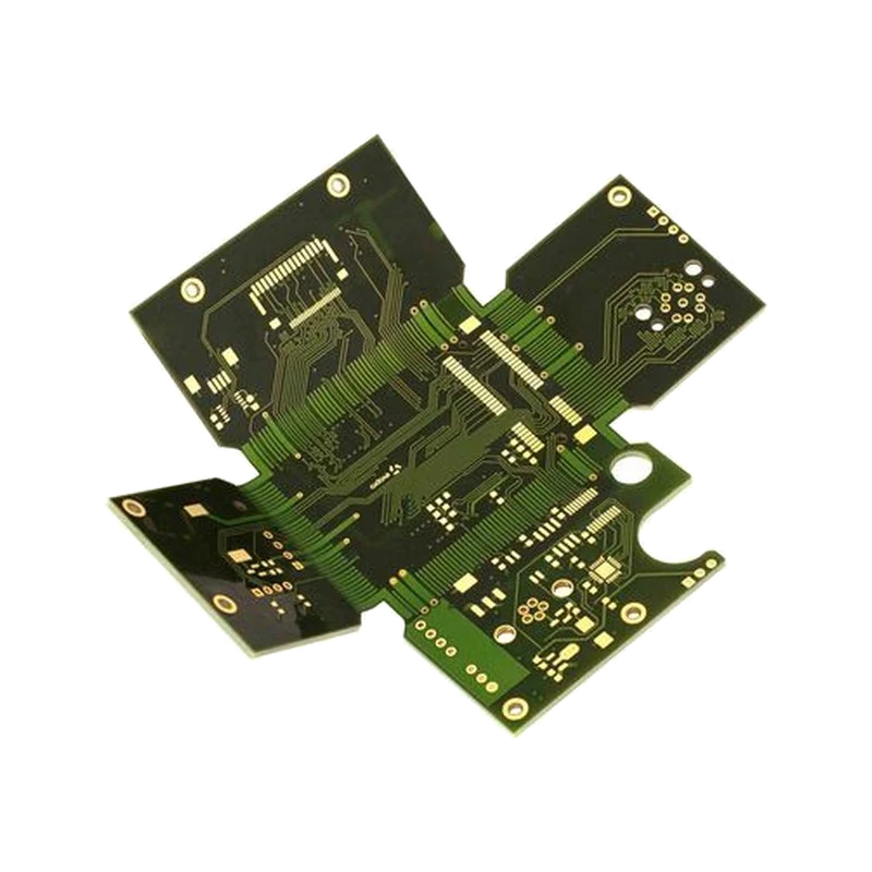
Polyimide flex circuits and rigid-flex constructions. They remove cables and connectors, cut assembly steps, and keep working through repeated bending.

  • Polyimide (PI) base material
  • Single-sided, double-sided and multilayer flex
  • Rigid-flex with multilayer rigid sections
  • Stiffeners and shielding on request

Rigid-Flex construction

Rigid section Flex bend area Rigid section

Multilayer rigid sections joined by a flexible polyimide bend area — no connectors, no cables, fewer solder joints.

🔬

HDI PCBs

High-density interconnect boards with laser-drilled microvias and sequential lamination, for designs where component density and layer count both have to go up.

  • 1 – 5 HDI build-up stages
  • 6 stages and above assessed case by case
  • Microvias and fine-pitch routing
  • Minimum trace / space / annular ring 75 µm

HDI microvia structure

Laser microvia Buried via L1 L2 L3 L4

Laser-drilled microvias and buried vias allow denser routing without adding layers — up to five sequential build-up stages.

📡

High-Frequency & High-Speed PCBs

Low-loss laminates and controlled-impedance stack-ups for RF, microwave and high-speed digital designs, where signal integrity has to hold up in production and not just in simulation.

  • PTFE and ceramic-filled materials
  • Rogers laminates (for example RO4350B)
  • Controlled-impedance stack-ups
  • Impedance test coupons on request
📚

Multilayer PCBs & Backplanes

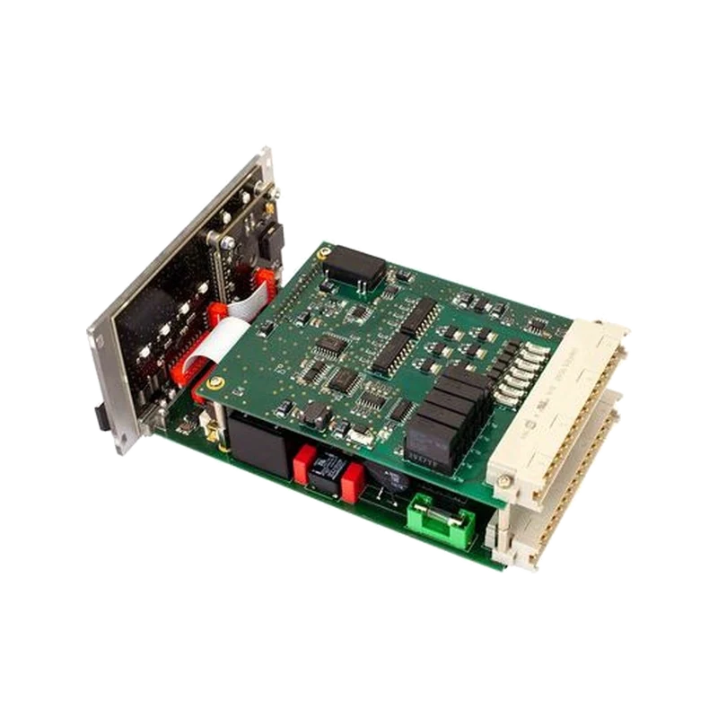
High layer counts with tight layer-to-layer registration and controlled impedance, including large-format panels for backplane and rack applications.

  • Up to 36 layers
  • Maximum panel size 21 × 33 inch
  • Controlled impedance
  • Heavy copper up to 12 oz on outer layers
🔧

PCB Assembly

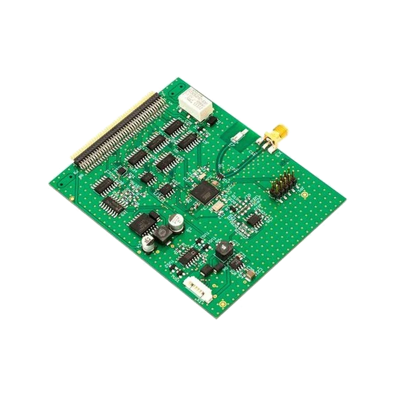
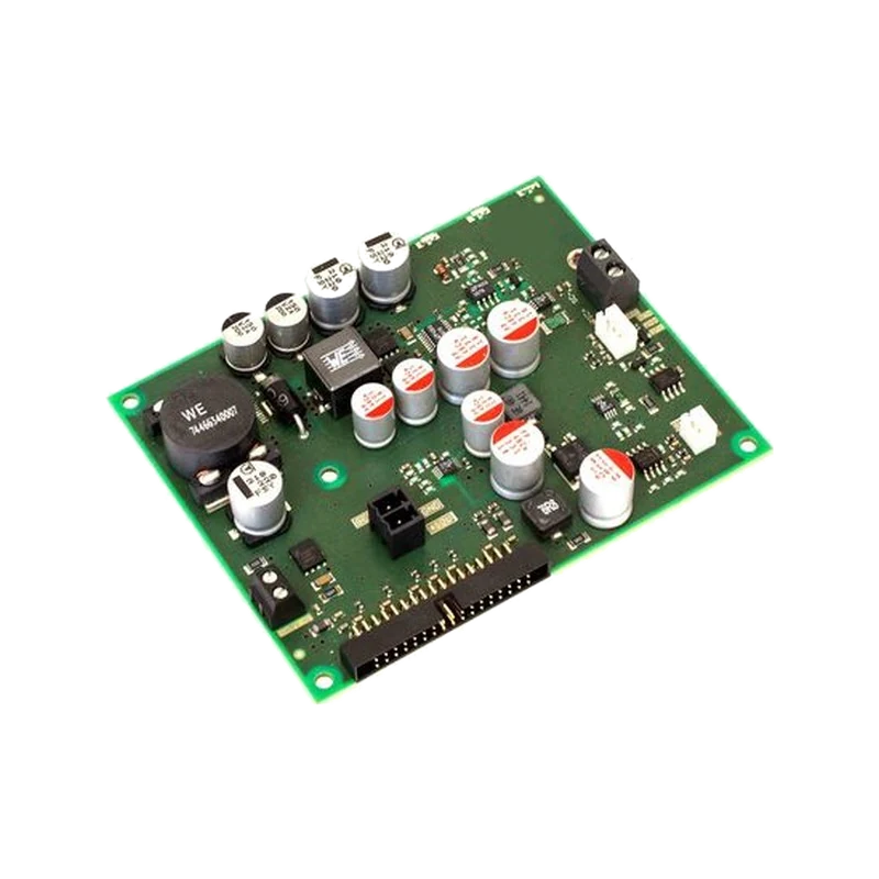
Turnkey SMT and through-hole assembly with component sourcing and hard-to-find part procurement, so you receive a finished board rather than a bare one.

  • SMD down to 01005 packages
  • BGA down to 0.6 mm, fine pitch to 0.4 mm
  • Any through-hole component type
  • Customer-supplied parts accepted
Additional Services

Beyond bare board fabrication

📐

Engineering Review

We check your data and stack-up before production and flag anything that would raise cost or hurt yield.

🧩

Component Sourcing

Standard and hard-to-find components sourced as part of an assembly order, with manufacturer names declared.

🚚

Quick-Turn Prototypes

12 hours for a 2-layer board and 24 hours for 4 layers, so a design change does not cost you a week of schedule.

Need a price for a specific board?

Send your Gerber files or a simple specification and we will come back with a quote within 12 hours.